What is Pump-Probe Microscopy?
Understanding semiconductors at the nanoscale is becoming increasingly important as electronics and photonics continue to shrink since nanoscale defects and structural features can have an outsized impact on the bulk electronic and optical properties of a nano-to-microscale device. For instance, defects can affect the diffusion lengths and lifetimes of the electrons and holes in a material, both of which are important characteristics in devices ranging from microelectronics to photovoltaics.
To disentangle how defects and structures change the electron and hole lifetimes in nanomaterials, researchers use numerous different characterization techniques (see Studying Nanomaterials: Spatial Resolution). One such technique, which allows researchers to isolate nano-to-microscale structural features, is called pump-probe microscopy. This technique involves two laser beams: (1) a pump beam that excites electrons from the conduction band into the valence band and (2) a probe beam that detects changes in the amount of transmitted or reflected light caused by the excited electron and hole population. By focusing these laser beams down to a nano-to-microscale spot, researchers can isolate and probe individual structures in a material.
Pump-probe microscopy is a spatiotemporal technique that typically involves two different experiments: (1) transient experiments and (2) imaging experiments.
(1) Transient Experiment
(1) Transient experiments. These involve changing the time delay between the pump and probe pulses in order to study the recombination rate at one spot on a material. In these experiments, there is a spike in the signal when the pump and probe are temporally overlapped due to an increase or decrease in the amount of transmitted probe light caused by the excited electrons and holes. The signal then exponentially decays away in time as the excited electrons and holes recombine. This decay in the signal can then be correlated to the recombination rate of the electrons and holes in the material.
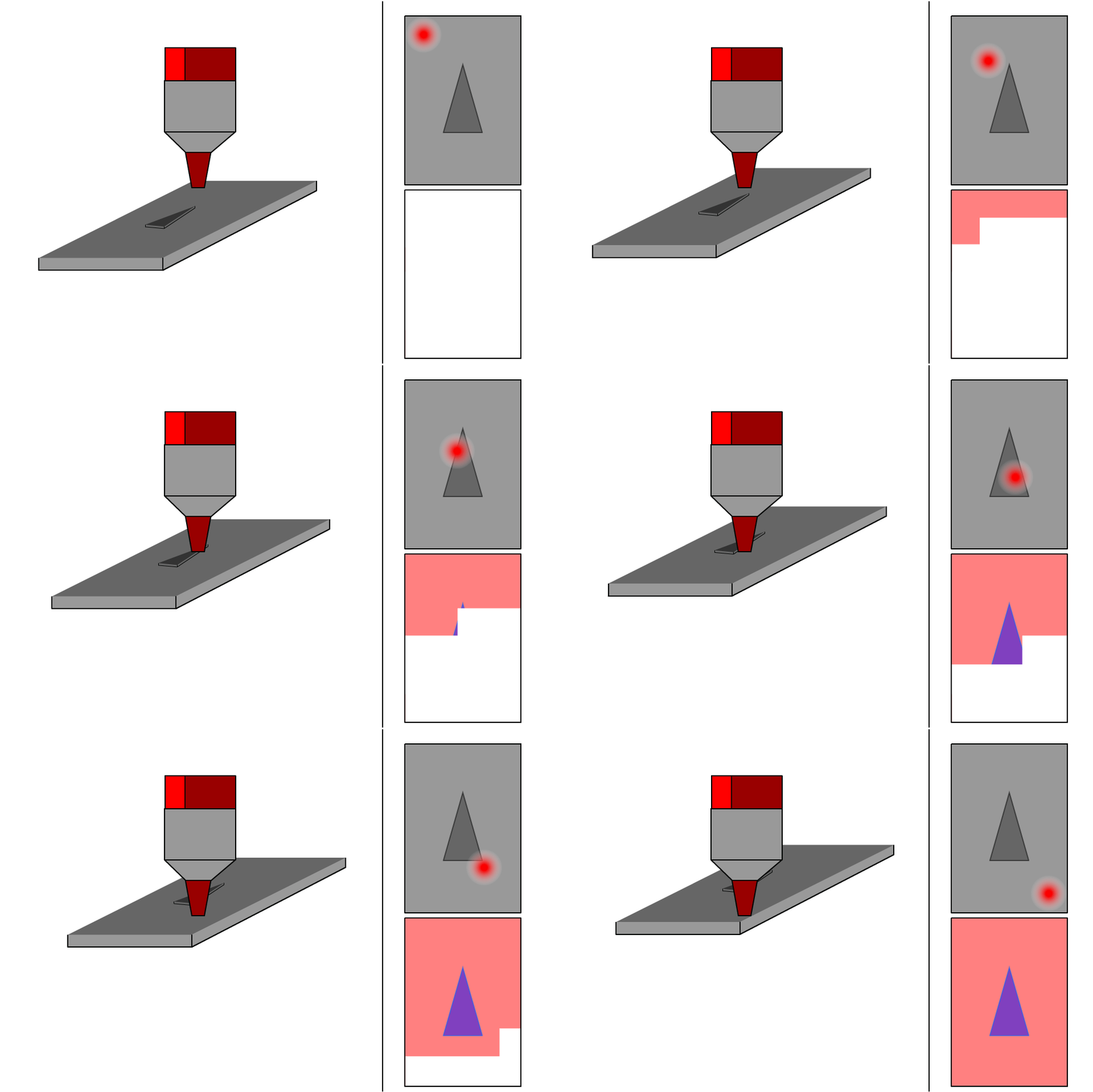
(2) Imaging experiments. These involve keeping the time delay between the pump and probe constant and scanning them across a material to create images that highlight structurally induced changes to the rate of electron and hole recombination.
Using this technique, researchers can determine how different structural features (such as edges, buckles, and tears) change the electronic properties of a material. Using this information, they can then optimize the structure of a material to target specific functionalities, such as slower recombination rates or faster diffusion rates, that are useful in specific device architectures.

